Seu Carrinho
Não existem mais produtos no seu carrinho


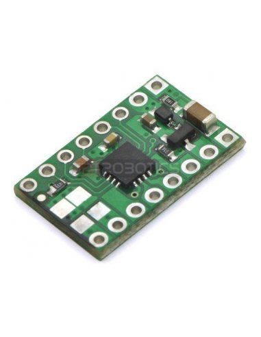


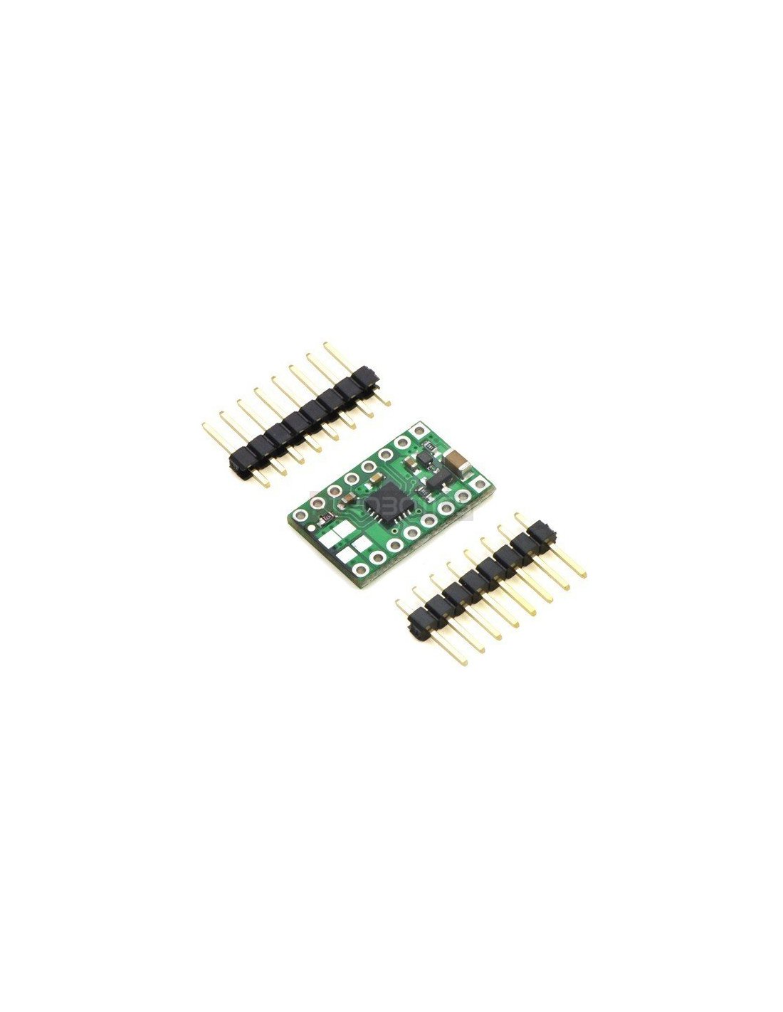
This tiny breakout board for TI’s DRV8833 dual motor driver can deliver 1.2 A per channel continuously (2 A peak) to a pair of DC motors.
This tiny breakout board for TI’s DRV8833 dual motor driver can deliver 1.2 A per channel continuously (2 A peak) to a pair of DC motors. With an operating voltage range from 2.7 to 10.8 V and built-in protection against reverse-voltage, under-voltage, over-current, and over-temperature, this driver is a great solution for powering small, low-voltage motors.
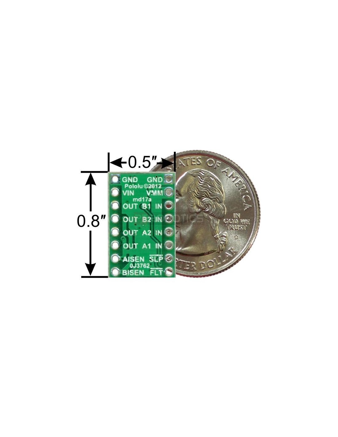
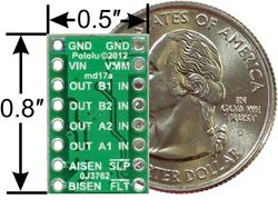  |
| DRV8833 dual motor driver carrier, bottom view with dimensions. |
|---|
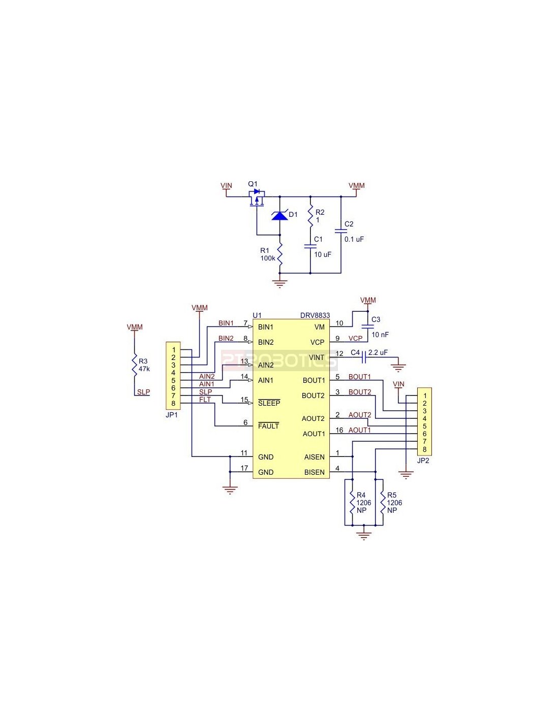
Texas Instruments’ DRV8833 is a dual H-bridge motor driver IC that can be used for bidirectional control of two brushed DC motors at 2.7 to 10.8 V. It can supply up to about 1.2 A per channel continuously and can tolerate peak currents up to 2 A per channel for a few seconds, making it an ideal driver for small motors that run on relatively low voltages. Since this board is a carrier for the DRV8833, we recommend careful reading of the DRV8833 datasheet (1MB pdf). The board ships populated with SMD components, including the DRV8833, and adds a FET for reverse battery protection.
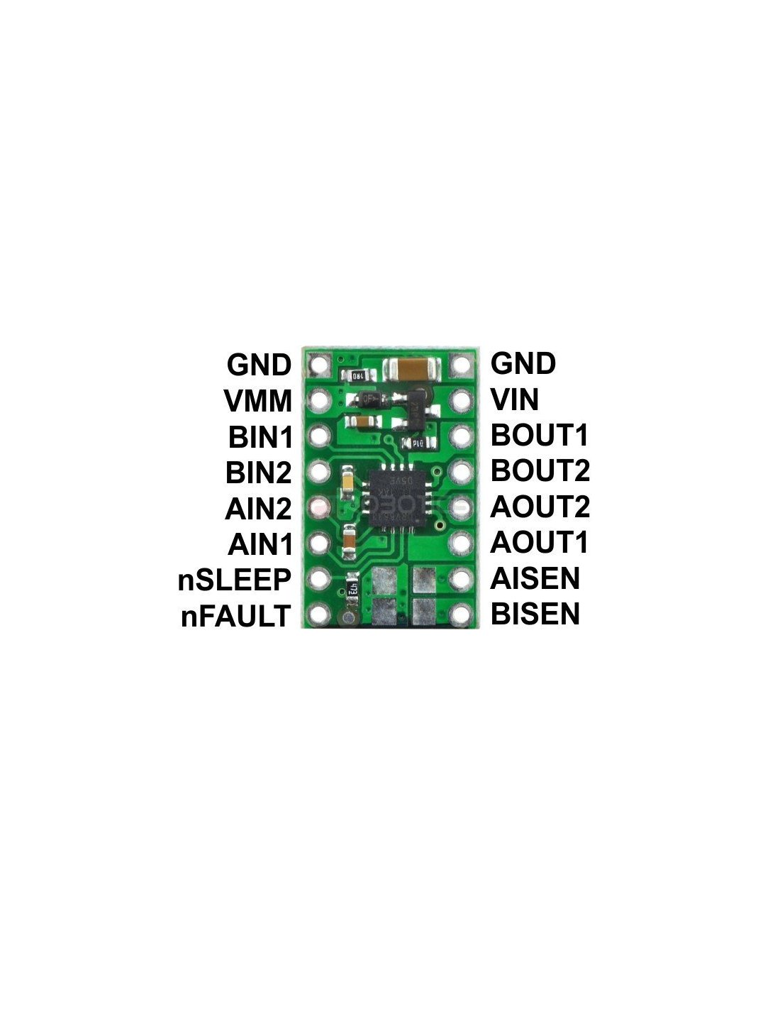
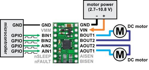 |
| Minimal wiring diagram for connecting a microcontroller to a DRV8833 dual motor driver carrier. |
|---|
In a typical application, power connections are made on one side of the board and control connections are made on the other. The nSLEEP pin is pulled high on the board and can be left disconnected if you do not want to use the low-power sleep mode of the DRV8833. Each of the two motor channels has a pair of control inputs, xIN1 and xIN2, that set the state of the corresponding outputs, xOUT1 and xOUT2; pulse width modulated (PWM) signal can be applied to each of these inputs. The control inputs are pulled low internally, effectively disabling the motor driver outputs by default. See the truth tables in the DRV8833 datasheet for more information on how the inputs affect the driver outputs.
The nFAULT pin is an open-drain output that is driven low by the chip whenever an over-current, over-temperature-or under-voltage condition occurs. Otherwise, it remains in a floating state, so you will need to connect an external pull-up resistor (or use a microcontroller input with its built-in pull-up enabled) if you want to monitor fault conditions on the driver.
 |
| PIN | Default State | Description |
|---|---|---|
| VIN | 2.7–10.8 V motor power supply connection. Operation with VIN below 5 V slightly reduces the maximum current output. | |
| VMM | This pin gives access to the motor power supply after the reverse-voltage protection MOSFET (see the board schematic below). It can be used to supply reverse-protected power to other components in the system, but it should not be used for high currents. This pin should only be used as an output. | |
| GND | Ground connection point for the motor power supply. The control source and the motor driver must share a common ground. | |
| AOUT1 | The motor A output pin controlled by AIN1. | |
| AOUT2 | The motor A output pin controlled by AIN2. | |
| BOUT1 | The motor B output pin controlled by BIN1. | |
| BOUT2 | The motor B output pin controlled by BIN2. | |
| AIN1 | LOW | The logic input control of AOUT1. PWM can be applied to this pin. |
| AIN2 | LOW | The logic input control of AOUT2. PWM can be applied to this pin. |
| BIN1 | LOW | The logic input control of BOUT1. PWM can be applied to this pin. |
| BIN2 | LOW | The logic input control of BOUT2. PWM can be applied to this pin. |
| nSLEEP | HIGH | Sleep input: when this pin is driven low, the chip enters a low-power sleep mode. (Labeled SLP on the board silkscreen.) |
| nFAULT | FLOAT | Fault output: driven low in the event of an over-current, over-temperature, or under-voltage condition; floating otherwise. (Labeled FLT on the board silkscreen.) |
| AISEN | Current sense pin for motor A. This pin is connected to ground and does not function by default, but current limiting can be enabled by making the modifications described below. | |
| BISEN | Current sense pin for motor B. This pin is connected to ground and does not function by default, but current limiting can be enabled by making the modifications described below. |
The DRV8833 can actively limit the current through the motors by using a fixed-frequency PWM current regulation (current chopping). By default, this carrier board connects the current sense pins to ground, disabling the current limiting feature. To enable current limiting, you can use a knife to cut the break points on the back of the board and then solder some appropriate current sense resistors to the unpopulated pads on the front, as indicated in the image below. The pads are sized for 1206 surface-mount resistors. Refer to the DRV8833 datasheet for information on how the resistor value determines the chopping current.
 |
The DRV8833 datasheet recommends a maximum continuous current of 1.5 A per motor channel. However, the chip by itself will overheat at lower currents. For example, in our tests at room temperature with no forced air flow, the chip was able to deliver 1.5 A per channel for about a minute before the chip’s thermal protection kicked in and disabled the motor outputs, while a continuous current of 1.2–1.3 A per channel was sustainable for many minutes without triggering a thermal shutdown. The actual current you can deliver will depend on how well you can keep the motor driver cool. The carrier’s printed circuit board is designed to draw heat out of the motor driver chip, but performance can be improved by adding a heat sink. Our tests were conducted at 100% duty cycle; PWMing the motor will introduce additional heating proportional to the frequency.


